- 您现在的位置:买卖IC网 > Sheet目录477 > MICRF506DEV1 (Micrel Inc)EVAL BOARD EXPERIMENTAL MICRF506
Micrel
MICRF506BML/YML
XCOtune
0
1
Start-up Time (μs)
590
590
VCO
A6..A0
0000011
D7
‘1’
D6
‘1’
D5
‘0’
D4
VCO_IB2
D3
VCO_IB1
D2
VCO_IB0
D1
VCO_freq1
D0
VCO_freq0
2
4
8
16
700
700
810
1140
The VCO has no external components. If has three
bit to set the bias current and two bit to set the VCO
frequency. These five bit are set by the RF
frequency, as follows:
31
2050
RF freq.
VCO_IB2
VCO_IB1
VCO_IB0
VCO_freq1 VCO_freq0
Table 7. Typical values with C EXT = 1.5pF
If an external reference is used instead of a crystal,
the signal shall be applied to pin 24, XTALOUT. Due
410MHz
410-423MHz
423-436MHz
436-450MHz
1
1
1
0
0
0
0
1
1
1
0
1
0
0
1
1
1
1
0
1
to internal DC setting in the XCO, an AC coupling is
recommended to be used between the external
reference and the XTALOUT-pin.
Table 8. VCO Bit Setting
The bias bit will optimize the phase noise, and the
frequency bit will control a capacitor bank in the
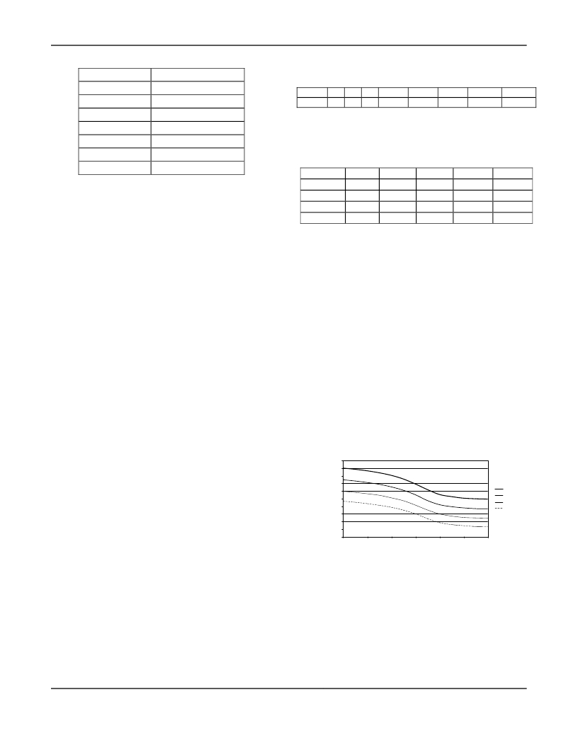
VCO. The tuning range, the RF frequency versus
varactor
voltage,
is dependent
on
the VCO
frequency setting, and can be shown in Figure 7.
When the tuning voltage is in the range from 0.9V to
1.4V, the VCO gain is at its maximum, approximately
32 to 35MHz/V. It is recommended that the varactor
voltage stays in this range.
The input capacitance at the varactor pin must be
taken into consideration when designing the PLL
loop filter. This is most critical when designing a loop
filter with high bandwidth, which gives relatively
small component values. The input capacitance is
approximately 6pF.
VCO frequency gain, Vdd=2.5V
480
470
460
450
440
430
420
410
400
390
380
11
10
01
00
0
0.4
0.8
1.2
1.6
2
2.4
V_varactor [V]
Figure 7. RF Frequency vs. Varactor Voltage
and VCO Frequency bit (V DD = 2.25V)
July 2006
17
M9999-092904
+1 408-944-0800
发布紧急采购,3分钟左右您将得到回复。
相关PDF资料
MICRF507YML TR
TXRX FSK LOW PWR W/AMP 32MLF
MICRF600DEV1
KIT DEV RADIOWIRE 902-928MHZ
MK01-C
SENSOR REED SPST-NO SMD
MK01-H
SENSOR REED SPDT-CHANGE SMD
MK02/0-1A66-500W
SENSOR REED SPST-NO
MK02/6-0
SENSOR REED PCB 24MM T/H
MK03-1C90C-500W
SENSOR REED SPDT CYLINDER
MK05-1A66C-500W
SENSOR REED SPST-NO SCREW MOUNT
相关代理商/技术参数
MICRF506DEV1
制造商:Micrel Inc 功能描述:KIT MICRF506 EVALUATION
MICRF506YML
制造商:Micrel Inc 功能描述:410/450MHZ ITRANSCEIVER SMD MLF32 制造商:Micrel Inc 功能描述:410/450MHZ ITRANSCEIVER, SMD, MLF32 制造商:Micrel Inc 功能描述:MICRF506 Series 410-450 MHz ISM Band FSK Transceiver - MLF-32 制造商:Micrel Inc 功能描述:410/450MHZ ITRANSCEIVER, SMD, MLF32; Frequency Min:410MHz; Frequency Max:450MHz; Modulation Type:FSK; Sensitivity dBm:-113dBm; Data Rate:200Kbps; Supply Voltage Min:2V; Supply Voltage Max:2.5V; RF IC Case Style:MLF; No. of Pins:32; ;RoHS Compliant: Yes
MICRF506YML TR
功能描述:射频收发器 410MHz to 470MHz, 2.0V to 2.5V, Low-Power FSK Transceiver with +10dBm Power Amplifier
RoHS:否 制造商:Atmel 频率范围:2322 MHz to 2527 MHz 最大数据速率:2000 Kbps 调制格式:OQPSK 输出功率:4 dBm 类型: 工作电源电压:1.8 V to 3.6 V 最大工作温度:+ 85 C 接口类型:SPI 封装 / 箱体:QFN-32 封装:Tray
MICRF506YMLTR
制造商:Micrel 功能描述:433MHz ISM Band Transceiver
MICRF506YML-TR
功能描述:IC RF TxRx Only General ISM < 1GHz 410MHz ~ 450MHz 32-VFQFN Exposed Pad, 32-MLF? 制造商:microchip technology 系列:- 包装:剪切带(CT) 零件状态:有效 类型:仅限 TxRx 射频系列/标准:通用 ISM < 1GHz 协议:- 调制:FSK 频率:410MHz ~ 450MHz 数据速率(最大值):200kbps 功率 - 输出:11dBm 灵敏度:-113dBm 存储容量:- 串行接口:SPI GPIO:- 电压 - 电源:2 V ~ 2.5 V 电流 - 接收:8mA ~ 12mA 电流 - 传输:8mA ~ 21.5mA 工作温度:-40°C ~ 85°C 封装/外壳:32-VFQFN 裸露焊盘,32-MLF? 标准包装:1
MICRF507
制造商:MICREL 制造商全称:Micrel Semiconductor 功能描述:470MHz to 510MHz Low-Power FSK Transceiver with 10dBm Power Amplifier
MICRF507YML TR
功能描述:射频收发器 470MHz to 510MHz, 2.0V to 2.5V, Low-Power FSK Transceiver with +10dBm Power Amplifier
RoHS:否 制造商:Atmel 频率范围:2322 MHz to 2527 MHz 最大数据速率:2000 Kbps 调制格式:OQPSK 输出功率:4 dBm 类型: 工作电源电压:1.8 V to 3.6 V 最大工作温度:+ 85 C 接口类型:SPI 封装 / 箱体:QFN-32 封装:Tray
MICRF507YMLTR
制造商:MICREL 制造商全称:Micrel Semiconductor 功能描述:470MHz to 510MHz Low-Power FSK Transceiver with +10dBm Power Amplifier
